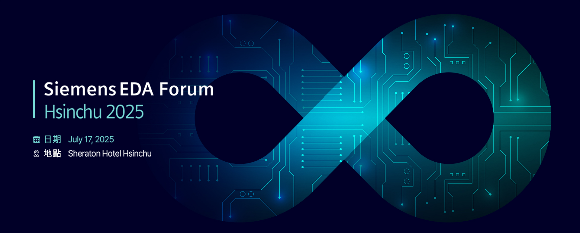
生成式 AI 加速半導體產業邁向軟體定義與智慧設計新時代,設計驗證流程與系統整合面臨前所未有的挑戰與轉機。Siemens EDA Forum 2025 匯聚產業領袖與技術專家,深入探討 AI 驅動的設計創新。
CEO 主題演講|Are We Ready? Succeeding in an AI-Driven, Software-Defined World
Siemens EDA CEO Mike Ellow 將分享如何運用完整的數位孿生架構,應對 AI 帶來的設計與運算挑戰,加速系統驅動、軟體定義的晶片創新。
分論壇主題 — 下午場分論壇延續熱門議題,從設計、驗證、製造到封裝,全面聚焦 AI 加值下的設計挑戰與創新解法五大分論壇,涵蓋:
09:00 |
Registration |
|---|---|
09:30 |
Welcome openingNina Lin, Vice President, GM Taiwan & PacRim South, Siemens EDA |
Are We Ready? |
|
From Cloud to Edge: Building the Future of AI, Together.Will Abbey, Executive Vice President and Chief Commercial Officer, Arm |
|
Investment Opportunities in AI: Semi/ Hardware/ etc.Jonah Cheng, Chief Investment Officer, J&J Investment Co., Ltd. |
|
11:10 |
Breakout session introductionLincoln Lee, VP Applications Engineering PacRim, Siemens EDA |
11:30 |
Lunch Break & Booth Tour |
In 2011, Marc Anderssen remarked that "software is eating the world". While software has been eating the world, AI is now rewriting the entire menu—transforming not just what we consume, but how it's created, served, and experienced.
This transformation is creating unprecedented demand for computational resources, with AI workloads driving exponential growth in compute infrastructure requirements. In response, a new wave of software innovation is emerging to orchestrate, optimize, and manage these increasingly complex computational ecosystems—fueling unprecedented demand for semiconductors in our software-defined, silicon-enabled global economy.
Organizations worldwide are making substantial investments in software development capabilities to navigate this transformation. However, electronic development teams face formidable challenges: scaling limitations at the physical level, multi-domain design complexities, fragmented data links across system integration layers, and a thinning engineering workforce amidst growing talent scarcity.
Successfully addressing these obstacles requires leverage of a comprehensive digital twin that goes beyond simulation and embraces a multi-faceted approach: implementing production-grade AI tools, establishing robust requirements capture methodologies, and enabling seamless software/hardware co-design processes. As traditional chip scaling approaches physical constraints, advanced packaging technologies like chiplets and 3D IC design workflows become essential. Cross-domain data management within the silicon lifecycle must connect with broader platforms while preserving domain-specific insights. Strategic partnerships with foundries and service providers round out this comprehensive strategy for enabling responsive, software-driven design processes.
In this presentation, Mike Ellow, CEO of Siemens EDA, will unveil Siemens' unique approach to maximize the possibilities of the digital twin for semiconductor & electronic design. By leveraging the most comprehensive digital twin framework for electronic systems, organizations can achieve the agility and integration needed to thrive in this new era of System-Driven-Systems Aware design—where software intelligence and silicon performance converge to create unprecedented capabilities and opportunities.

Chief Executive Officer, Siemens EDA
Mike Ellow is CEO, Siemens EDA Silicon Systems, Siemens Digital Industry Software, a business unit of Siemens Digital Industries. He leads Siemens EDA (formerly Mentor Graphics) Integrated Circuit Solutions (ICS) R&D, as well as EDA Global Sales. Ellow has led Siemens EDA Sales since August 2014 and Siemens EDA ICS R&D since 2023. He brings 30 years of executive sales and technical management experience, along with a proven track record of building strong sales and engineering teams while delivering positive, predictable results. These results are built on a foundation of focusing on customer success.
Ellow joined Mentor Graphics in March 2014 as part of the company's acquisition of Berkeley Design Automation, where he was Vice President of Worldwide Sales. Prior to that, he held various positions at Cadence Design Systems, overseeing sales in North America, Europe, and India, culminating in the role of Corporate Vice President, North American Sales. Prior to Cadence, he held management, marketing, and engineering positions in a number of different industries. He started his career as an electrical engineer at Hughes Aircraft.
Ellow has a BSEE from Lehigh University, an MSEE from the University of Southern California, and an MBA from California State University, Fullerton.
AI is no longer a distant promise - it's already reshaping how we work, live, and connect. And as this shift accelerates, one thing is clear: the choices we make now about how and where AI runs will shape the future for years to come.
From cloud to edge, we need solutions that are efficient, secure, and built to scale. That means rethinking architectures, reimagining deployment models, and coming together across the ecosystem. Whether you're designing silicon, developing software, or building the next wave of AI experiences, every layer of the stack has a role to play.
At Arm, we're working alongside you to drive this transition. Our shared goal: an AI ecosystem that thrives - one that spans chip designers, software developers, platform providers, and the innovators bringing intelligence to life. It's this collaboration that will unlock AI's full potential to transform industries, communities, and lives.
Join Will Abbey, Arm's Chief Commercial Officer, for a look at how we turn possibility into progress and why this moment, and this community, matter more than ever.

Executive Vice President and Chief Commercial Officer, Arm
Will leads sales, field engineering, and partner enablement at Arm, helping some of the world's most innovative organizations leverage the newest technologies to ready themselves for the next wave of digital transformation. From IP to AI, Will's unique insight has helped the world's technology leaders transform their products and operations.
Will joined Arm in 2004 and has held a number of leadership roles, including General Manager of Arm's Physical Design group. Before joining Arm, he worked in product management positions at Celoxica, Infineon Technologies, and Loughborough Sound Images. He serves on the board of EnPro Industries and holds a BEng from Sheffield Hallam University, UK.
As artificial intelligence continues to reshape industries, semiconductor and hardware innovation remain at the core of enabling future AI breakthroughs. Jonah will highlight key investment opportunities across AI-related semiconductor technologies, advanced hardware architectures, and next-generation designs.

Chief Investment Officer, J&J Investment Co., Ltd.
Jonah Cheng has been engaged in semiconductor research for more than 20 years and is currently the Chief Investment Officer of J&J Investment Co., Ltd. He previously served as an analyst at Merrill Lynch and as the Head of Semiconductor Research for Asia Pacific at UBS Securities. Jonah holds a bachelor's degree in Applied Chemistry from National Chiao Tung University and a Master of Business Administration degree from National Taiwan University.
As part of the foundational IP that helps build large digital designs, the use of standard cell IP significantly impacts digital design flows significantly. Standard cell libraries are fundamental in integrated circuit design, as they form the building blocks that implement all logic functionality in the final design, as well as ensure power, performance, and area (PPA) metrics are met.
This presentation explores a library-focused IP validation, selection, and generation approach from Solido, integrating Liberty model (.lib) PPA comparisons, visualization, analysis, with machine learning and smart technologies.
We’ll cover specifically the quality assurance aspect of IPs, and what makes IPs easier to integrate, making them more beneficial in terms of chip design schedule predictability. Alongside this, we’ll explore the potential of ML methodologies for libraries, especially when faced lack of data and tight schedules.
By effectively leveraging these technologies and considerations, chip architecture and design teams can make informed decisions about IP selection earlier, improving the quality and efficiency of SoC designs, and gaining a competitive edge in the market.

Technical Product Manager, Siemens EDA
Siddharth Ravikumar is a seasoned professional with over 13 years of experience in the semiconductor industry. He has a strong background in front-end design, verification, and test engineering. Currently, he serves as a Technical Product Manager for Solido IP Validation at Siemens EDA, where he applies his expertise to develop and launch innovative products. Siddharth holds a Master's degree in Electrical Engineering from Santa Clara University.
In today’s SoC design landscape, Design IP is delivered across multiple interdependent views such as logical, timing, physical, and electrical, and it continuously evolves across versions. Undetected inconsistencies between these views or regressions between IP revisions can result in late-stage design failures, costly ECOs, and delayed tapeouts.
This session presents a production-proven approach to comprehensive IP Validation using the Solido IP Validation Suite, which combines Solido Crosscheck for multi-view validation and IPdelta for version-to-version comparison. The suite enables early detection of structural mismatches, missing data, and cross-format errors well before integration and signoff, ensuring a consistent and reliable IP release at every iteration.
Through real-world examples, we will demonstrate how teams can scale IP Validation across all IP types and technologies, accelerate delivery, and achieve first-pass silicon success with confidence.
Technical Product Manager, Siemens EDA
Siddharth Ravikumar is a seasoned professional with over 13 years of experience in the semiconductor industry. He has a strong background in front-end design, verification, and test engineering. Currently, he serves as a Technical Product Manager for Solido IP Validation at Siemens EDA, where he applies his expertise to develop and launch innovative products. Siddharth holds a Master's degree in Electrical Engineering from Santa Clara University.
Siemens mPower provides power integrity for digital, analog and 3DIC across all types of design flows, at any scale. Siemens collaborates with ALi Corporation to share mPower experience of analog flow.
Application Engineer, Siemens EDA
Xiang Fang joined Siemens EDA as an application engineer in 2015. He is experienced in foundry tape-out flow optimization for years. Xiang currently focuses on helping customer to optimize the deisgn flow by leveraing Siemens shift-left products.
Deputy Technical Manger, ALi Corporation
Shan-You Chen is Deputy Technical Manager at ALi Corporation, leading advanced IC design flow development, CAD automation, and layout verification across multiple process nodes (UMC/TSMC 12–40nm). With over 15 years of semiconductor experience—including roles at Phison, Ilitek, and Nanya—he has deep expertise in high-speed circuit layout, mixed-signal design, and process automation. Chen is highly skilled with industry-standard EDA tools (HSPICE, Spectre, Cadence, Calibre) and scripting (Perl, TCL, SKILL), consistently enhancing quality and efficiency in project delivery. He holds an MS in Computer Science and Information Engineering from National Sun Yat-Sen University.
With increasing demands on power, performance, area, and yield in today’s IC designs, the need for accurate SPICE-level verification that includes process, voltage, temperature (PVT), and local variation has grown significantly. This ensures the quality and robustness of the final silicon. Traditional brute-force Monte Carlo solutions often fail to scale with these escalating design requirements. However, an effective SPICE-level verification methodology can meet these demands, delivering higher verification accuracy in a fraction of the runtime compared to traditional approaches.
This session will discuss how to achieve high accuracy and coverage for variation-aware verification at 3, 4, 5, and 6+ sigma targets in a comprehensive environment for analog design and verification, and how the latest Solido Additive Learning technology speedup verification for incremental and iterative workflows by 3X-20X.

Technical Product Manager, Siemens EDA
Lih Jen Hou is a Technical Product Manager at Siemens EDA for Analog and Mixed-signal circuit simulation products. He has over 10 years of experience in the Semiconductor industry with analog design roles in IC development, and pre/post sales application engineering in semiconductor foundry and EDA segments industry. He is currently focused on product marketing of next-generation EDA technologies with Siemens EDA’s Custom IC Verification Division, leveraging his design and customer engagement experiences. He has an M.S. in NanoEngineering from National TsingHua University.
Solido GenAI is set to transform the landscape of Custom IC design and verification with its groundbreaking Generative and Agentic AI capabilities to accelerate IC development, boost productivity, and bring your vision to market faster than ever. This innovative technology is uniquely tailored to each phase of the custom IC development process, from architecture exploration through prototyping to post-design workflows. It empowers engineering teams to achieve orders of magnitude productivity gains by automating complex verification processes through intuitive natural language interactions and applying sophisticated reasoning to quickly identify and resolve complex IC development challenges.
Join us in discovering how Solido GenAI’s innovative functional capabilities are revolutionizing IC design and verification. From automated setups to intelligent debugging, from advanced data mining to automated reporting, we're redefining what's possible in IC development. Experience firsthand how our integrated solution is helping engineers achieve new heights of design excellence.
Solido GenAI is set to transform the landscape of Custom IC design and verification with its groundbreaking Generative and Agentic AI capabilities to accelerate IC development, boost productivity, and bring your vision to market faster than ever. This innovative technology is uniquely tailored to each phase of the custom IC development process, from architecture exploration through prototyping to post-design workflows. It empowers engineering teams to achieve orders of magnitude productivity gains by automating complex verification processes through intuitive natural language interactions and applying sophisticated reasoning to quickly identify and resolve complex IC development challenges.

Senior Director, Siemens EDA
Sathish currently leads the product management and marketing organization for Custom IC Verification (CICV) division at Siemens. Sathish is an experienced product leader with over 20+ years of experience in EDA industry. Sathish’s focus is on bringing value to semiconductor ecosystem through innovative solutions. Sathish is proficient in scaling product portfolio growth and expansion of market share/revenue through relentless focus on data-based execution and thought leadership. Prior to Siemens, Sathish held various product management, strategic business development and corporate development roles for Cadence Design Systems and Synopsys. Sathish received his BS in Electronics & Communication from University of Madras, MS in computer engineering from University of Alabama & MBA from UC Berkeley- Hass School of Business.
The semiconductor industry is experiencing unprecedented growth, and this growth comes with significant challenges—more design starts, rising design complexities, shorter time-to-market, and a shrinking talent pool. To address these challenges, semiconductor companies are turning to AI-powered EDA solutions. While mainstream AI & GenAI technologies have seen rapid consumer adoption, adapting these AI technologies for EDA use cases is not straightforward due to stringent quality requirements for semiconductor design.
Ideally, EDA AI solutions that provide productivity boosts to chip designers and engineers should (a) seamlessly analyze design and verification data, (b) optimize complex processes, and (c) generate better designs. Across these functional areas, we will discuss illustrative ML, GenAI, and Agentic approaches. Additionally, we will also discuss the challenges associated with AI adoption, including data availability, model interpretability, and computational demands.
Further, we will discuss the grand vision of having a purpose-built centralized EDA AI system. Such a system framework can be very powerful by combining sophisticated foundational models or even IC domain-specific foundational models with a multimodal data lake to bring GenAI capabilities to push the boundaries of semiconductor innovation, paving the way for more efficient, scalable, and intelligent design processes.
Join us to explore the capabilities of EDA AI and see what the future holds!
Senior Director, Siemens EDA
Sathish currently leads the product management and marketing organization for Custom IC Verification (CICV) division at Siemens. Sathish is an experienced product leader with over 20+ years of experience in EDA industry. Sathish’s focus is on bringing value to semiconductor ecosystem through innovative solutions. Sathish is proficient in scaling product portfolio growth and expansion of market share/revenue through relentless focus on data-based execution and thought leadership. Prior to Siemens, Sathish held various product management, strategic business development and corporate development roles for Cadence Design Systems and Synopsys. Sathish received his BS in Electronics & Communication from University of Madras, MS in computer engineering from University of Alabama & MBA from UC Berkeley- Hass School of Business.
Alphawave Semi is pioneering high-speed connectivity IP solutions that drive next-generation compute and networking infrastructure across key growth markets such Data Center, AI, 5G/6G, and Storage.
Alphawave Semi's technology enables data centers and the world’s technology infrastructure to manage the exponential growth of data and prevent networking bottlenecks, with increasing volumes of data traveling faster, more reliably, and with higher performance at lower power. Alphawave Semi is a leader in the shift to chiplet-based System-on-Chip (SoC) architectures and our intellectual property (IP), custom silicon, connectivity products and chiplets are deployed by global tier-one customers across multiple sectors.
Alphawave Semi will showcase groundbreaking innovations through the session covering these technologies including 112G/224G PAM4 SerDes, Chiplets, UCIe D2D, PCIe, etc.

VP & Country Manager, APAC, Alphawave SEMI
Samuel Mao (毛存聖) is Vice President and Country Manager of Asia-Pacific (APAC) region of Alphawave Semi. Samuel joins Alphawave Semi with more than 25 years of semiconductor industry experience. Samuel has led Alphawave Semi APAC team since June 2024. Prior to joining Alphawave Semi, Samuel worked for several multi-nation companies like Marvell/Inphi, Mediatek, Broadcom/NetLogic, Asus, Vitesse, etc. with Sales, Marketing, AE/FAE, and RD different roles. He started his career as a SW/FW engineer at Hsinchu. Samuel holds a Master of Electrical Engineering and Computer Science from National Chiao Tung University in Taiwan. Samuel is willing to share with you the high performance, valuable connectivity IP solutions that Alphawave Semi brings to you to address the needs in the HPC, AI, Enterprise, High Speed Networking space during the speaker session.
Catapult AI NN is a complete solution that starts with a neural network description from an AI framework, converts it into C++ and synthesizes it into an RTL accelerator in Verilog or VHDL for implementation in silicon.

Application Engineer, Siemens EDA
Tim Hsu is a seasoned engineer with 18 years of experience in the IC design industry. He holds a Master's degree in Electrical Engineering from National Sun Yat-sen University in Taiwan. He has developed extensive expertise in various areas, including IP software and hardware development, co-verification, artificial intelligence, and FPGA design. He is currently a senior application engineer for Catapult High-Level Synthesis at SIEMENS EDA.
Designers face enormous challenges for low-power designs. Whether IoT at the edge, AI in the datacenter, robotics, or ADAS, the demand for increased functionality in SoCs is rapidly outpacing the power budget. Power must be considered at every chip design stage, including performance, reliability, and packaging. Waiting to address power until late in the design cycle – post-netlist or during physical implementation – can be extremely costly. The design may overrun the power budget, overheat, or have long-term reliability issues that cannot be addressed at the gate level, layout, or package selection. The best point in the design cycle to address power is at the beginning during the architectural and RTL stages. The earlier power analysis and optimization start, the more likely a chip will meet its power objectives. In this session, a low power methodology is presented to reduce the RTL power consumption progressively along the RTL development cycle.

Product Engineering Manager, Siemens EDA
Mohammed Fahad works with Siemens EDA as Product Engineering Manager. Fahad has 20 years of work experience in the field of Low Power, CDC and FPGA based system design. At Siemens EDA, Fahad is responsible for Low Power technology deployment and proliferation activities across a variety of Semiconductor customer base.
Tessent Embedded Analytics offers the only commercially available core agnostic RISC-V trace solution and provide small RTL modules, embedded directly in your SoC, which allow non-intrusive observation of what’s happening in your design when operational software is running on the system.
Application Engineer Manager, Siemens EDA
Jeff Fan (范熾東) is Taiwan and ASEAN (台灣及亞太區) Application Engineer Manager for the Tessent product family at Siemens EDA. Jeff has over 20 years of experience in various DFT aspects with respect to hierarchical flows and architectures including Scan, Memory / Logic BIST, Diagnosis. Jeff has been Tessent support engineer for more than 12 years and lots of support experience in different kind of DFT designs.
In this session, details of the latest new Questa One AI-driven capabilities will be revealed.

Questa Product Line Director, Siemens EDA
Moses Satyasekaran is the Simulation Product Line Director at Siemens EDA, bringing over two decades of experience in functional verification and simulation. He leads the evolution of the Questa portfolio, focusing on enabling intelligent simulation, functional safety, and verification management. Moses is passionate about helping engineering teams streamline verification workflows, improve productivity, and meet the growing demands of complex SoC and system design.
In many market segments, software-driven products that contain artificial intelligence are scaling rapidly and changing the nature and use of SoCs and the systems that contain them. This phenomenon brings unprecedented challenges to chip design and verification. In this presentation we define the Veloce ecosystem and the unique capabilities offered by the Siemens Veloce CS and Innexis platforms. The combination of these two platforms provides a broad foundation that transforms the design and verification flow and accelerates product development while reducing risk. The Veloce ecosystem, combined with other tools and technologies, addresses all aspects of design and verification from early in the design cycle to pre-silicon validation.
Sr. Director, Product Management, Siemens EDA
Vijay Chobisa has over 20 years of experience in hardware emulation. He is currently the Product Management Senior Director for Hardware-assisted Verification at Siemens EDA. He has worked as a technical marketing engineer and technical marketing manager at IKOS systems and as an ASIC design engineer at Logic++. Vijay holds a bachelor’s degree of electronics and communication engineering from Jai Narayan Vyas University, Rajasthan, India.
Questa One VIP enhances protocol verification by offering flexible topology support and easy-to-integrate, portable testbench code. With plug-and-play Compliance Test Suites, users can quickly perform thorough testing. Avery leads the industry with early support for PCIe Gen7, UCIe 2.0, and HBM4. Paired with Siemens’ Questa Simulator, it enables powerful Protocol-Aware Debug for efficient and high-quality verification.

Technical Support Engineer, Siemens EDA
Jimmy is a Technical Support Engineer responsible for front-end design and verification in the Asia-Pacific region. His main responsibilities include Verification IP (VIP), simulation verification and formal verification, as well as the development of new AI/ML based verification technology. He is dedicated to assisting clients in resolving various challenges they encounter during the design and verification process and providing efficient technical support to ensure their designs can smoothly pass verification and achieve the desired outcomes.
The collaboration between Siemens Innexis and AWS accelerates chip design using a "Shift-Left" methodology. This approach allows software development on a cloud-based virtual platform before physical silicon is ready. Critically, Innexis ANA runs natively on AWS Graviton (Arm-based) processors to achieve high-speed simulation, which significantly reduces time-to-market and lowers development risks.

Software Architect, Siemens EDA
Marco Liu is a Senior Application Engineer for the Hardware-assisted Verification (HAV) solutions at Siemens EDA. Marco has over 23 years of experience in various embedded software aspects, with deep expertise in system architecture for both Linux and Real-Time Operating Systems (RTOS). Drawing from his foundational experience as a Linux Engineer at MontaVista and a Platform Leader at Garmin, Marco now specializes in enabling automotive customers to apply shift-left principles and leverage cloud technologies to accelerate their complex software development cycles.

Sr. Solutions Architect, Amazon Web Services
Kage Yang currently serves as a Sr. Solutions Architect at AWS Taiwan, with over 10 years of experience in the IT industry. He primarily supports semiconductor and high-tech manufacturing companies, dedicated to helping enterprises plan and implement cloud solutions, and building secure, high-performance, flexible, and cost-effective environments on AWS.
Time-to-market matters. Calibre Vision AI enhances not only processing speed but also streamlines rule violation reviews through intelligent, human-like result analysis—saving time and effort.

Senior Application Engineer, Siemens EDA
With over a decade of experience in Calibre software applications, combining practical expertise in advanced processes from both semiconductor foundries and IC design companies, Frances serves as a Senior Application Engineer at Siemens EDA. In this role, she is responsible for promoting Calibre-related products, providing technical support, and serving as a course instructor.
Design teams face continuous challenges today to deliver power, performance, and area (PPA) metrics while balancing increasing design complexity and shorter design cycles. Traditional RTL-to-GDS methodologies require manual iteration with limited visibility into PPA tradeoffs, and produce results not easily transferrable to new or updated designs.
The chip design industry needs a smarter, faster, and more systematic approach that empowers engineering teams to consistently meet aggressive tapeout schedules, while retaining flow optimization and best practices to accelerate future designs.
This session covers how Aprisa with built-in AI capabilities redefines RTL-to-GDS methodologies to maximize productivity to PPA, delivering best practices and know-how directly to design teams, while leveraging optimal starting points to systematically explore and execute the best digital implementation solution for a given design.

Director, Product Management, Siemens EDA
Wei Lii Tan is Director of Product Management at Siemens DI SW’s Digital Design Creation Platform division, leading the product management and marketing team for the Aprisa RTL-to-GDS solution. Wei Lii has 20 years of experience in semiconductor and EDA, delivering solutions that help designers achieve faster, more efficient design closure through innovative new technologies. He has a master’s degree in electrical engineering from Mississippi State University, and an M.B.A. from Santa Clara University.
As the process becomes more advanced and the design more complex, verification cycles are getting longer and more difficult, making time-to-market increasingly stressful.Calibre provides a decisive advantage by reducing iteration and debug time by minimizing the rules and data required for DRC in early design stage. In addition, Calibre can help overcome physical server limitations to enable large-scale parallel data processing. These significantly reduces overall verification time and dramatically boosts design efficiency, making it a powerful to strengthen your product’s market competitiveness.
Application Engineer, Siemens EDA
Lucia is an Application Engineer for Calibre products at Siemens EDA. She works closely with customer to resolve various advanced-node tape-out issue and provides optimized design solution. Through these experiences, she has built a strong technical foundation and developed the ability to simplify complex challenges while delivering efficient solutions.
As advanced packaging and heterogeneous integration become key enablers in overcoming the limitations of traditional scaling, efficient 3DIC design and verification flows are more critical than ever.
This presentation introduces two essential technologies from Siemens EDA—Innovator3D IC and Calibre 3DSTACK—and how they enable a seamless 3Dblox-based path from system planning to physical signoff in complex 2.5D/3DIC designs.

Application Engineer, Siemens EDA
Responsible for Xpedition IC packaging software and 3DSTACK. Support customers in establishing 2.5D/3D IC verification processes, as well as solutions for High-Density Advanced Packaging (HDAP) and physical layout of package substrates.
Calibre's multiphysics verification solutions are designed to mitigate the complex interplay between thermal impacts and electrical behavior in 3D IC designs, helping design teams optimize their productivity while improving design quality.
Application Engineer Consultant, Siemens EDA
Oland is an Application Engineer Consultant at Siemens EDA, bringing over 15 years of experience in the semiconductor industry. His core competencies include physical verification, architectural performance optimization, and workflow streamlining. Oland excels at translating complex customer requirements and usage scenarios into customized Calibre solutions that enhance design robustness, accelerate time-to-market, and improve engineering productivity.
Product Specialist, Siemens EDA
Eddy Lu specializes in 3D-IC solutions at SEDA, covering Innovator 3DIC, Xpedition packaging design tools, Calibre 3DSTACK and 3DThermal. He has extensive experience supporting customers in developing 2.5D/3DIC verification flows to ensure system connectivity, completing the physical layout of advanced Fan-out RDLs, interposers, and substrate designs. In addition, Eddy actively supports chip-level thermal analysis for 3DIC designs, helping customers address thermal challenges early in the design cycle.
This section introduces a feature-based ML platform -- Calibre SONR that provides a machine learning approach for layout analysis and hotspot prediction, which serves both fabless and fab customers. SONR is a feature-based engine that by incorporating different design and process features, uses unsupervised, semi-supervised, and supervised ML models to build up flows like layout comparison to find the similarity/difference between layouts, layout reduction for down-sampling purposes, hotspot prediction for discovery hotspots and perform feature analysis for root cause analysis.

Application Engineer, Siemens EDA
Chieh-Hsun is an Application Engineer responsible for OPC verification and the evaluation and promotion of new ML tools. He is currently focusing on supporting OPC verification for TSMC’s advanced process nodes and helping to troubleshoot various issues arising from their production lines. He also works with TSMC to explore and assess potential applications of new ML tools in the process.
This section presents a holistic framework for Silicon Lifecycle Management (SLM) that addresses the increasing complexity of modern semiconductor devices throughout their entire lifespan. Tessent SLM framework integrates advanced telemetry through Tessent embedded analysitic monitors, or 3rd party PVT monitor IPs with IEEE 1687 ijtag interface together with High-Bandwidth IJTAG solution to provide unprecedented visibility into chip behavior and performance characteristics.
Application Engineer Manager, Siemens EDA
Jeff Fan (范熾東) is Taiwan and ASEAN (台灣及亞太區) Application Engineer Manager for the Tessent product family at Siemens EDA. Jeff has over 20 years of experience in various DFT aspects with respect to hierarchical flows and architectures including Scan, Memory / Logic BIST, Diagnosis. Jeff has been Tessent support engineer for more than 12 years and lots of support experience in different kind of DFT designs.
Unlike High-Bandwidth IJTAG introducing in previous section, This section will introduce a SSN different usage scenario and allow user reuse SSN bus to deliver generic data.
Application Engineer Consultant, Siemens EDA
With over 10 years of hands-on experience in the DFT (Design for Test) field, Ivan has been dedicated to this domain since his student days. He has previously held key positions at TSMC (Taiwan Semiconductor Manufacturing Company) and MTK (MediaTek), gaining extensive industry experience. Currently, Ivan works as an Application Engineer at Siemens EDA, where he focuses on providing advanced Electronic Design Automation (EDA) solutions to clients and continues to
This section will present in-system deterministic test methodology specifically designed to identify and characterize aging-induced defects in semiconductor devices. In-system deterministic test, In-System TestKompress (ISTK) functionality enables you to use the Tessent™ Streaming Scan Network (SSN) software to generate and retarget patterns through the In-System Test (IST) controller, or MissionMode controller. The recommended protocol for delivering scan data is through the SSN parallel bus. This manual describes the enhanced functionality for using ISTK
with the parallel bus.

Senior Application Engineer, Siemens EDA
Wei Hsuan Yang is a Senior Application Engineer for Tessent at Siemens EDA, with prior experience at MediaTek and MStar. He has a solid background in semiconductor design and verification, and specializes in applying DFT methodologies to optimize testability and performance in advanced SoC designs.
Scan chain diagnosis has been used to identify systematic defect mechanism during yield ramp. Electrical failure analysis techniques like Laser Voltage Probing/Imaging (LVX) are essential for further isolating potential defect locations to guide precision physical failure analysis (PFA). However, due to the advanced nodes like back-side power, it makes optical fault isolation very challenging. It’s critical to have better fault isolation resolution through improved scan diagnosis for accelerating PFA. In this talk, we will discuss the high resolution scan chain diagnosis and other methods like pre-silicon analysis for improving diagnosis resolution. By adopting these new approaches, the number of single suspect chain diagnosis cases are increased significantly, benefitting PFA and time-to-market.

Foundry Program Engineer, Siemens EDA
Jim Yang is the foundry program engineer at Siemens EDA. He has collaborated closely with the foundries for developing robust design-for-test (DFT) flows including hierarchical DFT, innovative streaming scan network (SSN), 3DIC and diagnosis. Through successful DFT implementation on advanced nodes including 3D stacking test chips, Jim has helped the foundries and Siemens EDA to enable the ecosystem benefiting the industry. Jim was a DFT engineer for design service and DFT solution engineer in the EDA industry before joining Siemens EDA. Jim has expertise areas in DFT such as memory BIST, Scan, boundary scan and multi-die, and also full digital design flow like synthesis, timing analysis and validation. Jim holds a master degree of electrical engineering from National Central University.

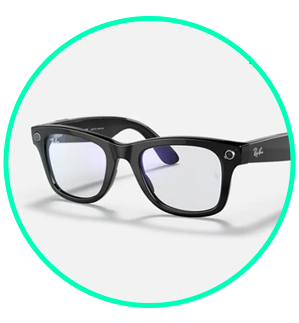
Nintendo 任天堂 Switch 2 與 Meta 雷朋智能眼鏡
活動當日課程結束後,只要填寫會後問卷,
西門子客製化手機磁吸支架
完成會場內所有展示攤位的互動集章活動,
7-11 CITY CAFE 提貨卡
填寫完整會後問卷即可獲得 咖啡券兌換券一張,


如有論壇相關問題請與Siemens EDA forum 活動小組連繫:2025eda@ace-event.com.tw